x




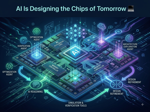
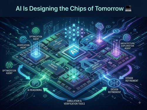
Artificial intelligence is no longer simply running on the world's most advanced chips. It is increasingly helping engineers design, verify and optimise those chips in the first place.
That shift could become one of the most important developments in the semiconductor industry. As modern processors become dramatically more complex — particularly AI accelerators, chiplets and 3D integrated circuits — traditional electronic design automation (EDA) workflows are under increasing pressure.
Siemens and NVIDIA are now pushing towards an AI-native approach to semiconductor engineering, in which AI agents can plan tasks, operate engineering software, analyse results and repeatedly verify their decisions. Rather than using AI merely as a clever assistant inside an individual application, the goal is to create autonomous systems capable of coordinating lengthy, multi-stage engineering workflows.
The significance is easy to miss. If successful, AI will not just consume increasingly powerful hardware. AI could help create the next generation of hardware that makes more powerful AI possible.
Designing a modern semiconductor is an extraordinarily complicated engineering challenge.
Today's processors can contain billions of transistors, sophisticated memory systems, high-speed interconnects and multiple specialised processing blocks. AI chips add another layer of complexity because designers are constantly balancing performance, power consumption, thermal behaviour, manufacturing constraints and cost.
Then there is verification.
Before a new chip reaches a manufacturing line, engineers need to establish that its architecture and implementation behave as intended. Errors discovered after fabrication can be extraordinarily expensive because fixing them may require a new silicon revision.
This makes verification one of the most time-consuming parts of the semiconductor development process. Siemens says verification can account for up to 70% of design time, illustrating why automation has become such an important target for AI.
The challenge becomes even greater as companies move towards AI accelerators, chiplet-based architectures and increasingly sophisticated 3D IC designs.
There is an important distinction between traditional AI-assisted EDA and the newer agentic AI approach.
An AI assistant might help an engineer write some RTL code, analyse a result or suggest a potential optimisation.
An AI agent is intended to go considerably further.
It can be given an engineering objective and then determine which tools it needs, execute multiple steps, inspect the results and adjust its approach. Multiple specialised agents can also collaborate on different parts of the same workflow.
Siemens' Fuse EDA AI Agent is designed around this concept. The system can orchestrate multi-tool and multi-agent workflows covering areas such as architectural exploration, RTL development, verification, physical implementation and manufacturing sign-off.
That represents a fundamental change in the way engineers could interact with EDA software.
Instead of manually moving between numerous specialised tools, an engineer could increasingly specify what needs to be achieved, while AI agents handle much of the process required to reach that objective.
The partnership between Siemens and NVIDIA brings together two complementary capabilities.
Siemens has decades of expertise in EDA software — the tools used by semiconductor engineers to design, simulate, verify and prepare chips for manufacturing.
NVIDIA brings specialised AI models, accelerated computing infrastructure and software technologies designed to support AI reasoning and agentic workflows.
Their expanded collaboration is focused on creating self-verifying AI agents for semiconductor and printed circuit board design.
The crucial word here is "verifying".
A generative AI model can produce an answer that looks convincing without necessarily being correct. That is particularly dangerous in chip engineering, where an apparently minor mistake can ultimately result in a defective design.
Siemens' approach is therefore to allow AI agents to continuously validate their decisions against deterministic, physics-based EDA engines. In other words, the AI does not simply decide that its work looks right; specialised engineering software is used to test whether the proposed solution actually satisfies the required constraints.
This creates a potentially powerful feedback loop:
AI reasons → engineering tools execute → results are measured → AI evaluates the results → the design is refined → verification continues.
That is much closer to an autonomous engineering workflow than conventional generative AI.
NVIDIA's contribution extends beyond simply providing GPUs.
The companies are integrating NVIDIA AI technologies including Nemotron models, CUDA-X libraries and NVIDIA's agentic AI infrastructure into Siemens' EDA environment. Siemens says these technologies are intended to improve reasoning, tool calling, token efficiency and the performance of long-running engineering workloads.
The partnership also involves NVIDIA's NeMo Gym framework for agentic environments and NVIDIA OpenShell for secure execution of autonomous agents.
This matters because an engineering agent needs more than a language model.
It needs access to tools.
It needs context.
It needs to understand specialised engineering data.
It needs to execute actions reliably.
And, perhaps most importantly, it needs mechanisms for determining whether those actions produced a valid result.
That is why the emerging AI-native EDA stack looks considerably different from simply adding a chatbot to existing chip-design software.
One of the most compelling applications is verification.
Engineers traditionally need to test designs against huge numbers of possible scenarios. As chip complexity rises, the number of potential states and interactions can become enormous.
AI agents could help explore this enormous design space more intelligently.
Instead of relying exclusively on engineers to identify which tests should be run next, an agent could analyse previous results, identify suspicious areas, generate additional tests and launch appropriate verification tools.
Siemens and NVIDIA say their latest approach allows agents to continuously validate their decisions against established engineering tools. The companies are targeting workflows capable of delivering sign-off-quality results much faster, with Siemens stating that accelerated computing can help move some workloads from days towards hours.
The potential impact is significant.
A faster verification cycle means engineers can test more ideas without necessarily extending the overall development schedule. That could encourage greater experimentation and allow problems to be discovered earlier.
Perhaps the most fascinating aspect of this development is the feedback loop it creates.
AI requires enormous amounts of computing power.
That demand drives the development of increasingly sophisticated processors.
Those processors are becoming harder and more expensive to design.
AI is now being introduced into the design process to help engineers cope with that complexity.
The resulting chips can then power more capable AI systems.
This creates a cycle in which AI helps build the hardware needed to advance AI itself.
Siemens explicitly describes this relationship in its partnership with NVIDIA, noting that its EDA tools and Fuse agentic capabilities can run on NVIDIA GPUs while NVIDIA technologies are also being incorporated into the EDA stack.
It is a fascinating example of technology becoming part of the process by which its own infrastructure evolves.
The ambition also extends beyond individual integrated circuits.
Siemens' Fuse EDA AI Agent is designed to work across semiconductor, 3D IC and PCB workflows. Its scope can extend from early architectural exploration and RTL coding through verification and physical implementation to sign-off and manufacturing readiness.
That broader approach could eventually transform semiconductor engineering from a collection of disconnected software tasks into a more coordinated, AI-orchestrated workflow.
Imagine an engineer specifying a set of requirements such as:
achieve a particular performance target;
stay within a defined power envelope;
support a particular manufacturing process;
meet thermal constraints;
minimise die area; and
satisfy stringent verification requirements.
An AI-native EDA system could potentially coordinate many of the steps required to explore those constraints.
It could propose architectural options, generate implementation details, run simulations, identify failures, modify the design and repeat the process.
Human engineers would still establish the goals, constraints and acceptance criteria, but much of the repetitive exploration could become automated.
Despite the excitement, it would be misleading to describe this as AI simply replacing chip designers.
Semiconductor engineering involves complex trade-offs, domain expertise, safety considerations and decisions that can have enormous financial consequences.
The more realistic near-term scenario is engineers working with increasingly autonomous digital colleagues.
AI agents can perform repetitive exploration and analysis at machine speed, while experienced engineers remain responsible for requirements, architecture, judgement and final sign-off.
That distinction is especially important because AI systems can still make mistakes.
A convincing AI-generated solution is not necessarily a correct engineering solution.
This is precisely why self-verification is becoming such an important part of the AI-native EDA concept.
The semiconductor industry cannot afford to treat AI-generated designs in the same way as AI-generated text.
If a chatbot produces an incorrect paragraph, the consequences may be minor.
If an autonomous agent introduces an error into a chip design, the consequences could include months of additional engineering work, expensive fabrication runs and delayed product launches.
There are also security concerns.
As AI agents gain access to sensitive chip-design data and increasingly powerful engineering tools, companies will need strong access controls, auditing and safeguards.
Siemens says its NVIDIA OpenShell integration is intended to provide governed execution environments with security controls and audit trails for autonomous agents.
Research is also beginning to examine the security implications of combining LLMs with EDA and modern chiplet architectures, highlighting the possibility of new attack surfaces within AI-driven hardware-design workflows.
In other words, the industry must solve two problems simultaneously:
How can AI design better chips?
And:
How can we prove that the AI's decisions can be trusted?
Siemens is not alone in pursuing agentic AI for chip development.
The wider EDA industry is moving rapidly towards systems capable of automating increasingly large portions of the semiconductor workflow. Siemens' latest announcements demonstrate how quickly the focus is shifting from individual AI-powered features towards long-running agents capable of coordinating multiple engineering tools.
The competitive stakes are enormous.
As semiconductor companies race to develop faster AI accelerators, CPUs, networking processors and custom silicon, the ability to shorten design cycles could become a major competitive advantage.
Even relatively small improvements can matter when a new generation of hardware may determine whether a company can keep pace with rapidly evolving AI workloads.
The most interesting question is not whether AI will be used in chip design. That is already happening.
The question is how autonomous these systems will become.
Today's AI-native EDA systems are moving towards agents that can plan, execute and verify complex workflows. The next stage could involve increasingly sophisticated multi-agent systems in which different AI specialists handle architecture, verification, optimisation, physical design and other tasks.
Human engineers may increasingly become orchestrators of these systems rather than manually performing every step themselves.
That does not mean the semiconductor engineer disappears.
Instead, the engineer's role could move further up the abstraction ladder — from individually executing thousands of design operations towards defining objectives, constraints and verification requirements while supervising increasingly capable AI systems.
The semiconductor industry has spent decades developing increasingly sophisticated automation tools. Agentic AI represents a potentially important next step: moving from software that performs predefined operations towards systems that can reason about engineering objectives and coordinate multiple tools to achieve them.
Siemens and NVIDIA's work is an important example of that transition.
Their vision combines specialised EDA software, accelerated computing, AI models and autonomous agents with deterministic engineering verification. If the technology delivers on its promise, semiconductor teams could explore far more design possibilities while reducing the time required to reach reliable results.
The implications extend well beyond chip companies.
Every smartphone, data centre, electric vehicle, industrial machine and AI system ultimately depends on semiconductor technology. If AI can make the process of designing those semiconductors faster and more efficient, the effects could ripple across the entire technology industry.
The most remarkable part may be what happens next.
AI is becoming a tool for designing the machines that will run the next generation of AI.
That could turn the semiconductor design process into one of the most important frontiers in the wider AI revolution.
For readers interested in the technology behind this development, Siemens' detailed overview of its Fuse EDA AI Agent explains how agentic AI is being applied across semiconductor and PCB design workflows.
Siemens has also published details of its expanded partnership with NVIDIA and the technologies being combined to support AI-native chip design, verification and manufacturing readiness.
Disclaimer: This article is provided for informational purposes only, mistakes may be made, and it's not offered or intended to be used as legal, tax, investment, financial, or any other advice.